|
2013年10月02日,總部設立於台灣竹科的Macronix International Co Ltd(旺宏電子;下稱旺宏)於美國維吉尼亞州地方法院,指控總部位於美國加州Spansion Inc. 及Spansion LLC(飛索半導體;下稱Spansion)之快閃記憶體相關產品,侵犯其專利權,要求合理的權利金、損害賠償以及支付訴訟律師費等。
本案可視為被告對原告的反擊,達到恐怖平衡的效果。起因於2013年8月1日,Spansion同時於美國加州北區地方法院及ITC提告,要求審理旺宏及其客戶之包含有記憶體的產品侵害其專利權,詳細內容及兩造背景介紹請參考本室於2013年8月15日之報導:記憶體專利訴訟Spansion控告旺宏電子及其客戶 Read.aspx?PostID=8528。
本案系爭專利共7項,涉及快閃記憶體晶片的製造、高效能串列式記憶體介面設計及記憶體單元的安全性及電路設計等,詳細資料整理如下:
- 美國專利編號US5,619,052,名稱為電子清除式可複寫唯讀記憶體設備的電極間介電質結構(Interpoly dielectric structure in EEPROM device),係於1994年9月29日申請,1997年4月8日核發,專利權人為Macronix International Co., Ltd.。
- 美國專利編號US5,836,772(與US5,619,052為同一專利家族),名稱為閘間層介電質程序(Interpoly dielectric process),係於1997年3月31日申請,1998年11月17日核發,專利權人為Macronix International Co., Ltd.。
- 美國專利編號US5,998,826,名稱為三向浮動閘極記憶體以及具備隔離通道的程式化、已程式化以清除程序的操作方法(Triple well floating gate memory and operating method with isolated channel program, preprogram and erase processes),係於1996年9月5日申請,1999年12月7日核發,專利權人為Macronix International Co., Ltd.。
- 美國專利編號US6,031,757,名稱為具備使用者可程式化區塊鎖定功能的寫入保護之非揮發性記憶體裝置(Write protected, non-volatile memory device with user programmable sector lock capability),係於1996年11月22日申請,2000年2月29日核發,專利權人為Macronix International Co., Ltd.。
- 美國專利編號US6,421,267,名稱為記憶體陣列架構(Memory array architecture),係於2001年4月24日申請,2002年7月16日核發,專利權人為Macronix International Co., Ltd.。
- 美國專利編號US8,341,324,名稱為用以資料傳輸的序列周邊介面(Serial peripheral interface and method for data transmission),係於2012年1月31日申請,2012年12月25日核發,專利權人為Macronix International Co., Ltd.。
- 美國專利編號US8,341,330,名稱為一種用於序列周邊介面增強讀取效能的方法與系統(Method and system for enhanced read performance in serial peripheral interface),係於2008年1月7日申請,2012年12月25日核發,專利權人為Macronix International Co., Ltd.。(1081字;表2)
表一、系爭專利解析
| US5,619,052 |
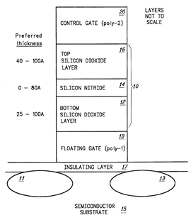
1. A dielectric insulating composite for insulating a floating gate from a control gate in a nonvolatile memory cell, the dielectric insulating composite comprising:
a bottom layer of silicon dioxide formed on said floating gate;
a layer of silicon nitride formed on said bottom silicon dioxide layer, said silicon nitride layer having a thickness which is less than said bottom silicon dioxide layer; anda top layer of silicon dioxide formed on said nitride layer, said top silicon dioxide layer having a thickness which is greater than said silicon nitride layer.
主要描述非揮發性記憶體區塊之浮動閘極與控制閘極間的介電質絕緣層結構 |
 |
| US5,836,772 |
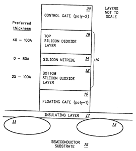
1. A process for fabricating a nonvolatile memory cell comprising:
a) forming source and drain regions on a first conductivity-type semiconductor substrate;
b) forming an insulating layer on said source and drain regions;
c) forming a floating gate positioned on said insulating layer;
d) forming a dielectric composite positioned on said floating gate, said dielectric composite including a bottom layer of silicon dioxide formed on said floating gate; a layer of silicon nitride formed on said bottom silicon dioxide layer, and a top layer of silicon dioxide formed on said nitride layer, wherein said silicon nitride layer of said composite has a thickness less than about 80 A and is thinner than said top or said bottom silicon dioxide layer; and
e) forming a control gate positioned on said dielectric composite.
描述非揮發性記憶體的製程 |
 |
| US5,998,826 |
1. A floating gate memory cell in a semiconductor substrate including a region having a first conductivity type, the first conductivity type being one of n-type and p-type, and wherein the substrate is coupled to an external reference supply applying a ground potential and a positive supply potential, comprising:
a first well within the region of the substrate having a second conductivity type, being one of n-type and p-type and different than the first conductivity type;
a second well within the first well, having the first conductivity type;
a drain within the second well, having the second conductivity type;
a source within the second well, having the second conductivity type, and spaced away from the drain to define a channel area between the drain and the source;
a floating gate structure disposed over the channel area and extending substantially from the source to the drain, including a floating gate and a tunnel insulator between the floating gate and the substrate;
a control gate structure over the floating gate, including a control gate and an insulator between the floating gate and the control gate; and
circuits to induce tunneling of electrons out of the floating gate into the channel area of the substrate by applying a positive voltage higher than the supply potential to the second well, a positive voltage to the first well, and a negative voltage to the control gate, while the region of the substrate is grounded.
描述浮動閘極式記憶體之組成架構 |
 |
| US6,031,757 |
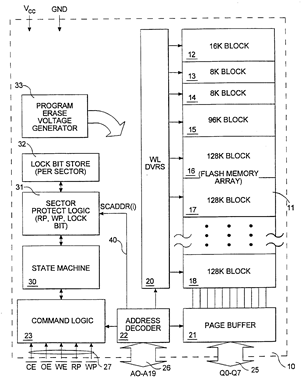
1. An integrated circuit memory, comprising:
an array of non-volatile erasable and programmable memory cells, including a plurality of sectors;
a plurality of control inputs for receiving a set of control signals;
address inputs for receiving address signals;
data input/outputs for transferring data into and out of the array;
command logic, coupled to the plurality of control inputs, and to at least one of the address inputs and the data input/outputs, which detects command sequences at the plurality of control inputs and the at least one of the address inputs and the data input/outputs, indicating operations for the array, including a program operation to program data in the array, a sector erase operation to erase a sector of the array, a read operation to read data in the array, and a sector lock operation to set a sector lock signal for at least one sector in the array;
sector protect logic coupled to the command logic, including non-volatile, sector lock memory which stores the sector lock signal for at least one sector in the array indicating a protect status for a corresponding sector in the array; which inhibits the sector erase and program operations in a particular sector in response to a set sector lock signal corresponding to the particular sector and to a first state of control signals in the set of control signals; and
erase, program and read circuits responsive to the command logic and the sector protect logic to execute the sector erase, program and read operations, and to execute the sector lock operation.
描述非揮發性可清除及可程式記憶體之區塊陣列及其信號傳輸與控制 |
 |
| US6,421,267 |
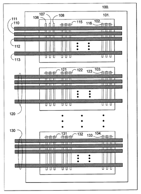
1. A memory array architecture, at least comprising:
a plurality of memory cells;
a plurality of select transistors connecting to the memory cells, wherein the select transistors include upper block select transistors and lower block select transistors; and
a plurality of bit lines connecting to the select transistors, wherein odd bit lines connected to the upper block select transistors are located in a first metal layer and even bit lines connected to the lower block select transistors are located in a second metal layer.
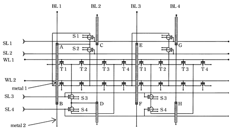
描述記憶體陣列架構 |
 |
| US8,341,324 |
1. A serial peripheral interface of an integrated circuit, the serial peripheral interface comprising:
a plurality of pins coupled to the integrated circuit, wherein:
the integrated circuit receives an instruction through only one of the plurality of pins;
after receiving the instruction through the only one pin, the integrated circuit receives an address through the plurality of pins in continuity with the receipt of the instruction; and
the integrated circuit sends read out data through the plurality of pin.
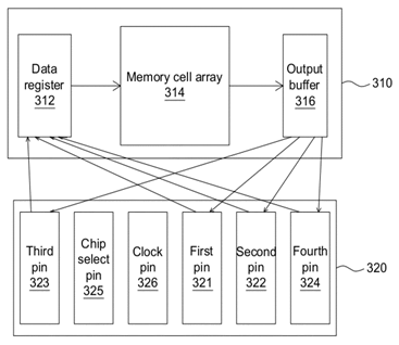
描述積體電路的資料傳輸的序列周邊介面 |
 |
| US 8,341,330 |
1. A method for conducting a read operation in an integrated circuit, the method comprising:
receiving a read command; receiving a first address in a clock cycle after receiving the read command; receiving a first performance enhancement indicator in a clock cycle immediately after receiving the first address while before starting to send data out, for determining whether an enhanced read operation is to be performed; and
performing the enhanced read operation, in case of determining that the enhanced read operation is to be performed.
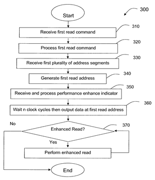
描述於積體電路執行讀取操作的方法 |
 |
表二、旺宏與Spansion相關專利訴訟案件基本資料:
| 訴訟名稱 |
Macronix International Co., LTD. v. Spansion Inc. et al |
Spansion LLC v. Macronix America Co., Ltd. et al |
Spansion LLC v. Macronix America Co., Ltd. et al |
| 提告日期 |
2013年10月02日 |
2013年8月1日 |
2013年8月1日 |
| 原告 |
Macronix International Co., LTD.
(旺宏電子股份有限公司) |
Spansion LLC |
Spansion LLC |
| 被告 |
Spansion Inc.; Spansion LLC.
(飛索半導體) |
Macronix America Co., Ltd.
Macronix America Inc.
Acer, Inc.
Acer America Corporation
Asustek Computer, Inc.
Asus Computer International
Belkin International, Inc.
D-Link Corporation
D-Link System, Inc.
Netgear Inc.,
Nintendo Co., Ltd.
Nintendo of America, Inc. |
Macronix America Co., Ltd.
Macronix America Inc.
Acer, Inc.
Acer America Corporation
Asustek Computer, Inc.
Asus Computer International
Belkin International, Inc.
D-Link Corporation
D-Link System, Inc.
Netgear Inc.,
Nintendo Co., Ltd.
Nintendo of America, Inc. |
| 案號 |
3:13-cv-00679-REP |
4:13-cv-03566-DMR |
337-TA |
| 訴訟法院 |
U.S. District Court for the Eastern District of Virginia |
California Northern District Court |
ITC |
| 系爭專利 |
US5,619,052;US5,836,772;
US5,998,826;US6,031,757;
US6,421,267;US8,341,324;
US8,341,330 |
US6,369,416;US6,900,124;
US7,018,922;US6,459,625;
US7,151,027;US6,731,536 |
US6,369,416;US6,900,124;
US7,018,922;US6,459,625;
US7,151,027;US6,731,536 |
| 系爭產品 |
NAND Flash Memory;
Nor Floating Gate Flash Memory;
Nor Flash Memory;
Nor Mirror Bit Flash Memory;
SPI Flash Memory; |
NOR Flash; Mask ROM;
Acer Laptop; Nintendo Wii; Router |
NOR Flash; Mask ROM;
Acer Laptop; Nintendo Wii; Router |
| 訴狀下載 |
 |
|
|
Source: 科技政策研究與資訊中心—科技產業資訊室整理,2013/10/14
|