| US 7,782,749請求項1 |
US 8,165,081請求項1 |
1. A method for mapping a plurality of Physical Downlink Control CHannels (PDCCHs) to resources in a wireless communication system, comprising:
一項用來在無線通訊系統中映射複數實體下行控制通道(PDCCHs)到資源的方法,包括 |
1. A method for a base station to assign to an user equipment (UE) communicating with the base station a number of coded control information symbols being transmitted with coded data information symbols during the same transmission time interval by the UE, the method comprising:
一項用來讓基地台可以分配一組經編碼之控制資訊符號給與該基地台進行通訊的用戶設備(UE),其在UE相同的傳輸間隔中與經編碼之資料資訊符號一併傳輸,該方法包括 |
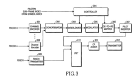
allocating, by a concatenator (Fig.3 - 302), at least one Control channel Element (CE) to each of the plurality of PDCCHs;
由串接器分配至少一個控制通道元件(CE)給複數PDCCHs中每個PDCCH |
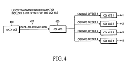
assigning, by the base station, an offset value to the UE;
由基地台分配一個偏移值給UE |
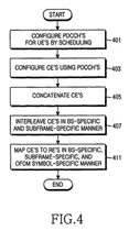
concatenating, by the concatenator, if at least one PDCCH is scheduled to be transmitted in a subframe, elements in the plurality of PDCCHs;
若至少一個PDCCH被排定以一子訊框來傳輸,由串接器串接複數PDCCHs中的元件 |
assigning, by the base station, a Modulation and Coding Scheme for data reformation (data MCS) (Fig.4 - 410) to the UE;
由基地台分配一資料重組之調變編碼機制(data MCS)給UE |
interleaving, by an interleaver (Fig.3 - 303), the concatenated elements; and
由一交錯器交錯複用前述被串接之元件 |
transmitting information regarding the offset value to the UE; and
傳輸有關偏移值之資訊給UE |
mapping, by a Control channel Elements (CE)-to-Resource Element (RE) mapper (Fig.3 - 306), the interleaved elements to at least one RE.
由一映射控制通道元件(CE)到資源元件(RE)之映射器,映射前述經交錯之元件到至少一個RE |
transmitting information regarding the data MCS to the UE, wherein the number of coded control information symbols assigned to the UE for transmission of control information is determined based on the data MCS and the offset value, and the control information comprises at least one of channel quality information (CQI), Acknowledgement (ACK)/Non-Acknowledgement (NAK), Precoding Matrix Index (PMI), and Rank Indicator (RI).
傳輸有關data MCS之資訊給UE,其中為了傳輸控制資訊而分配給UE之經編碼資訊符號的數量是基於data MCS與偏移值來決定,而控制資訊包含至少通道品質資訊(CQI)、確認(ACK)/未確認(NAK)訊息、與秩數指標(RI)其中之一 |
|
|
|
| US 8,208,438 請求項1 |
US 8,228,827 請求項1 |
1. A method for transmitting a downlink control channel in mobile communication system using Orthogonal Frequency Division Multiplexing (OFDM), the method comprising the steps of:
一項使用正交分頻多工(OFDM)在行動通訊系統中傳輸下行控制通道的方法,該方法包含以下步驟 |
1. A method for performing a random access procedure in a mobile communication system, the method comprising:
一項用來在行動通訊系統中進行隨機接入程序之方法,該方法包括 |
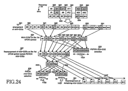
mapping the downlink control channel to Resource Elements (REs), wherein the downlink control channel comprises a plurality of RE groups;
映射前述下行控制通道到資源元件(REs),其中下行控制通道包含複數RE群組 |
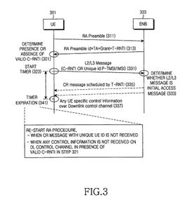
receiving a first message including a random access preamble (Fig.3 - 311);
接收包括隨機接入前文之第一訊息 |
transmitting downlink control information via the mapped downlink control channel;
透過前述經映射之下行控制通道傳輸下行控制資訊 |
transmitting a second message, which is a random access response message, in response to the first message (Fig.3 - 313);
傳輸第二訊息,其為一隨機接入回應訊息,以回應前述第一訊息 |
wherein each of the plurality of RE groups comprises four REs, and each RE group has a single time index; and
其中複數RE群組中個別群組由4個RE構成,且個別RE群組具備單一時間索引 |
determining whether or not a third message including a Cell-Radio Network Temporary Identifier (C-RNTI) is received from a User Equipment (UE)(Fig.3 - 333);
決定一包括基地台無線電網路暫時身分(C-RNTI)之第三訊息是否被接收自一用戶設備(UE) |
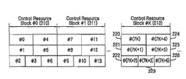
wherein the plurality of RE groups are allocated to available resources in the downlink control channel in a time first manner, wherein the available resources are divided into a two-dimensional frequency/time structure, and wherein, during allocation, a time index is increased from an initial value up to a predetermined value in a given frequency index, before increasing to a next frequency index and resetting the time index to the initial value.
複數RE群組以時間優先方式被分配給在下行控制通道中的可得資源,其中可得資源被區分成二維頻率/時間結構,而時間索引在一既定的頻率索引中從一起始值增加至一預設值,而後再增加至下一個頻率指引且時間索引被重新設定成預設值 |
transmitting a fourth message, which is a Contention Resolution (CR) message for the random access procedure (Fig.3 -335), to the UE, upon receipt of the third message that does not include the C-RNTI from the UE; and
在接收來自UE之不包括C-RNTI的第三訊息後,傳輸第四訊息至UE,其為用在前述隨機接入程序之競爭解決(CR)訊息 |
transmitting UE-specific control information to the UE (Fig.3 - 337), upon receipt of the third message including the C-RNTI from the UE, wherein the UE-specific control information includes a Cyclic Redundancy Check (CRC) specifically mapped to the C-RNTI of the UE, and wherein the first, second, third, and fourth messages occur in a random access procedure in a mobile communication system.
在接收來自UE之包括C-RNTI的第三訊息後,傳輸UE特定的控制資訊至UE,其中UE特定之控制資訊包括特別映射到UE之C-RNTI的循環冗餘校驗(CRC),以及在行動通訊系統裡隨機接入程序中所發生的第一、第二、第三與第四訊息 |
|
|
|
| US 6,617,929 請求項1 |
US 6,767,813 請求項1 |
|
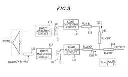
1. A microwave Doherty amplifier for inducing a Doherty operation, wherein quarter wave transformers (Fig.3 – 141 & 142) are connected to final outputs of a carrier amplifier (Fig.3 - 10) and a peaking amplifier (Fig.3 - 20) coupled in parallel to each other, the Doherty amplifier comprising:
一項用來導出Doherty技術操作的Doherty微波功率放大器,其中一四分之一波長轉換器被連接到、互相並聯之載波放大器與峰值放大器的最終輸出上,該Doherty放大器包括
|
1. A method of manufacturing an integrated circuit device, comprising:
一項用來製造積體電路裝置的方法,包括
|
|
a first load matching circuit (Fig.3 - 121) connected to an output terminal of the carrier amplifier so as to obtain a microwave output matching for an output impedance of the carrier amplifier;
第一負載匹配電路,其被連接到前述載波放大器的輸出終端,藉以取得一匹配載波放大器輸出阻抗之微波輸出
|
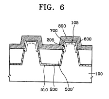
forming a trench (Fig.6 - 200) in a substrate (Fig.6 - 100);
在一基體上形成溝渠
|
|
a second load matching circuit (Fig.3 - 122) connected to an output terminal of the peaking amplifier so as to obtain a microwave output matching for an output impedance of the peaking amplifier;
第二負載匹配電路,其被連接到前述峰值放大器的輸出終端,藉以取得一匹配峰值放大器輸出阻抗之微波輸出
|
forming an isolation layer (Fig.6 – 500’) comprising an insulating material in the trench so as to cover a first sidewall portion of the trench and an entire bottom of the trench and to expose a second sidewall portion of the trench;
在溝渠中形成一由絕緣材料所構成之隔絕層,其包覆溝渠之第一側牆部分與全部底部,並暴露出溝渠之第二側牆部分
|
a first phase tuning component (Fig.3 - 131) for adjusting a phase of a first equivalent circuit including the carrier amplifier and the first load matching circuit to obtain an output matching for both real and imaginary parts of an output impedance of the first equivalent circuit, which is located behind the first load matching circuit; and
第一相位調諧組件,其位於前述第一負載匹配電路之後,用來調整包括前述載波放大器與前述第一負載匹配電路之第一等效電路的相位、並藉以取得與第一等效電路輸出阻抗之實部與虛部相匹配的輸出 |
forming an impurity layer (Fig.6 - 600) in the second sidewall portion of the trench; and
在溝渠第二側牆部分形成一摻雜層 |
a second phase tuning component (Fig.3 - 132) for adjusting a phase of a second equivalent circuit including the peaking amplifier and the second load matching circuit to obtain an output matching for both real and imaginary parts of an output impedance of the second equivalent circuit, which is located behind the second load matching circuit.
第二相位調諧組件,其位於前述第二負載匹配電路之後,用來調整包括前述峰值放大器與前述第二負載匹配電路之第二等效電路的相位、並藉以取得與第二等效電路輸出阻抗之實部與虛部相匹配的輸出 |
forming a gate electrode (Fig.6 - 800) on the second sidewall portion of the trench.
在溝渠第二側牆部分形成一閘極 |
|
|
|
| US 6,865,682 請求項1 |
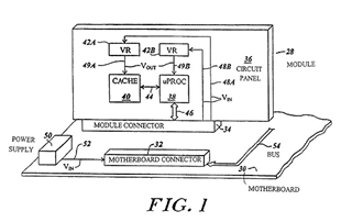
1. A processor module (Fig.1 - 28) comprising:
一項處理器模組,包括 |
a circuit panel (Fig.1 – 36);
一電路板 |
a processor (Fig.1 - 38) mounted to said circuit panel;
一處理器,被架設在前述電路板上 |
support electronics (Fig.1 - 40) for said processor mounted to said circuit panel in electronic communication with said processor;
用於前述處理器之支援電子元件,被架設在前述電路板上並導通於前述處理器 |
a voltage regulator mounted to said circuit panel in electronic communication with said processor and said support electronics, said voltage regulator for receiving an input voltage from a remote voltage source, for modifying the input voltage at the voltage regulator (Fig.1 – 42A & 42B) to generate a regulated output voltage, and for providing the regulated output voltage to said support electronics and said processor said voltage regulator comprising a switching voltage regulator that includes a feedback path for sensing at least one of a voltage level and current level of the regulated output voltage;
電壓調節器,被架設於前述電路板上並導通於前述處理器與前述支援電子元件,前述電壓調節器用來接收來自遠端電源之一輸入電壓、用來在電壓調節器上調整輸入電壓以產出經調解的輸出電壓、並用來提供經調節之輸出電壓給前述支援電子元件與前述處理器,前述電壓調節器由一個切換式電壓調節器所構成,其包括一用來感應至少一個電壓準位以及經調節輸出電壓之目前準位的回饋路徑 |
an interface (Fig.1 - 34) for removably coupling said circuit panel to a motherboard (Fig.1 - 30), said input voltage being at a fixed voltage level sourced at said motherboard, converted from an external power supply voltage at said motherboard, and provided to said circuit panel through said interface to said voltage regulator; and
用來可拆卸式耦接前述電路板至一母板上的介面,前述輸入電壓為一源自前述母板之固定電壓準位,在前述母板上從一外部電源供應電壓轉換而來,並透過前述介面被提供給前述電路板、進而給前述電壓調解器 |
a decoupling capacitance on the circuit panel in parallel with the voltage regulator for decoupling high-frequency components of current-time variance in the input voltage.
位在電路板上之解耦電容,其並聯於電壓調節器上,用來解耦在輸入電壓中現時變異的高頻部分 |
|
|