2015年11月05日,註冊於美國德拉瓦州的專利授權公司North Star Innovations Inc向美國德拉瓦州地方法院控告台灣的DRAM半導體製造商南亞科技公司(Nanya Technology Corporation)及其美國子公司(Nanya Technology Corp. USA)侵犯其US 5,892,777(下稱 '777號專利)、US 6,127,875(下稱'875號專利)、US6,157,583(下稱'583號專利)、US 6,372,638(下稱'638號專利)、US6,492,686(下稱'686號專利)五件DRAM電路專利。
圖一、DRAM半導體專利訴訟 North Star Innovations控告南亞科技

本案五件系爭議專利的原申請人均為美國通訊大廠Motorola Inc.,並由Motorola拆分出的子公司飛思卡爾半導體(Freescale Semiconductor)取得後,最後移轉至North Star Innovations。值得注意的是,該五件專利包含DRAM電路的監測、電壓轉換電路、保護電路、緩衝電路、製成方法等不同技術領域,從而增加被告防禦的困難度。本案五件系爭議專利如下:
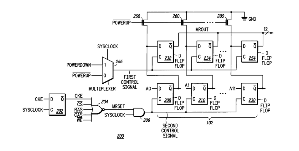
- '777號專利名稱為「觀察記憶體裝置之模式的設備及其方法(Apparatus and method for observing the mode of a memory device)」。
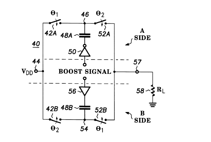
- '875號專利名稱為「互補式雙重加升電壓轉換器(Complimentary double pumping voltage boost converter)」。
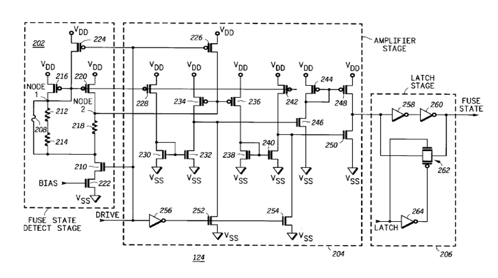
- '583號專利名稱為「具有一保險絲偵測電路的積體電路記憶體及其方法(Integrated circuit memory having a fuse detect circuit and method therefore)」。
- '638號專利名稱為「於積體電路的複數導電層之間,形成一個導電插件的方法(Method for forming a conductive plug between conductive layers of an integrated circuit)」,其另有US6,143,648與其同屬一專利家族。
- '686號專利名稱為「包含一個具擺盪率控制功能之緩衝電路的積體電路(Integrated circuit having buffering circuitry with slew rate control)」,且其另有US6,066,971與其同屬一專利家族。
本案原告North Star Innovations為一專利授權公司,自美國半導體大廠飛思卡爾半導體(Freescale Semiconductor)及Motorola取得23件專利。飛思卡爾於2004年由原摩托羅拉(Motorola)的半導體部門分拆成立,雖然2015年3月3日恩智浦半導體(NXP Semiconductors)收購了飛思卡爾,但是,並未取得所有專利資產,反而將部分專利移轉給North Star進行主張,以換取現金。
本案被告南亞科技公司為台塑集團旗下南亞塑膠轉投資公司,創立於1995年3月4日,於2000年8月17日,南亞科技於臺灣證券交易所股票上市(臺證所:2408)。其主要業務為動態隨機存取記憶體(DRAM)及晶圓代工,目前擁有一座八吋晶圓廠和一座12吋晶圓廠。其另與美光科技(Micron)合資成立華亞科技。
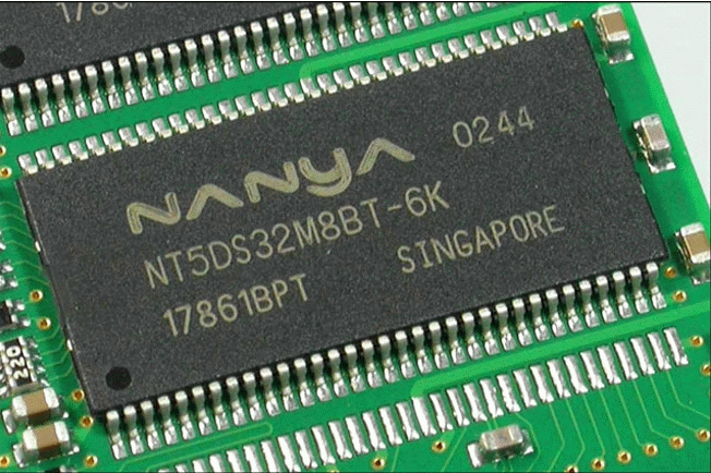
圖二、系爭產品--南亞DRAM晶片
原告於起訴狀陳稱被告生產、銷售之DRAM產品(包含但不限於)
- Nanya 512Mb LPDDR2-S4 SDRAM NT6TL16M32AQ/ NT6TL32M16AQ;
- NT5TU32M16DG-AC U57A 512 Mb DDR2SDRAM;
- NT5CC512M8BB-DI-V70A 4Gb DDR3 SDRAM;
- NT5CB64M16FP-DH DDR3 1Gbit SDRAM;
- NT5TU32M16DG-AC 512 Mb DDR2 SDRAM;
- NT6TL256F32AQ-G1 8 Gb Low-Power DDR2 SDRAM;
- NT5CC512M8BN-DI DDR3 SDRAM;
- NT5TU32M16DG-AC U57A 512 Mb DDR2SDRAM
使用了上述五件爭議專利保護之技術,且原告曾於2015年10月發函要求南亞科技取得其授權,惟雙方未達成共識,故請求法院判決原告確認被告侵權,要求其停止損害,並賠償原告之損失。(1082字;表11;圖1)
表一、專利訴訟基本資料表
| 訴訟名稱 |
North Star Innovations Inc. v. Nanya Technology Corp. U.S.A. et al |
| 提告日期 |
2015年11月05日 |
| 本案原告 |
North Star Innovations Inc. |
| 本案被告 |
Nanya Technology Corp. U.S.A.; Nanya Technology Corp. |
| 訴訟案號 |
1:15-cv-01027 |
| 訴訟法院 |
Delaware District Court |
| 系爭專利 |
US 5,892,777; US 6,127,875; US 6,157,583; US 6,372,638; US 6,492,686. |
| 爭議產品 |
- Nanya 512Mb LPDDR2-S4 SDRAM NT6TL16M32AQ/ NT6TL32M16AQ;
- NT5TU32M16DG-AC U57A 512 Mb DDR2SDRAM,
- NT5CC512M8BB-DI-V70A 4Gb DDR3 SDRAM
- NT5CB64M16FP-DH DDR3 1Gbit SDRAM;
- NT5TU32M16DG-AC 512 Mb DDR2 SDRAM,
- NT6TL256F32AQ-G1 8 Gb Low-Power DDR2 SDRAM
- NT5CC512M8BN-DI DDR3 SDRAM;
- NT5TU32M16DG-AC U57A 512 Mb DDR2SDRAM
|
| 訴狀下載 |
 |
表二、系爭專利資訊
| 專利名稱 |
Apparatus and method for observing the mode of a memory device |
| 公告號 |
US 5,892,777 |
| 申請號 |
US 08/851,287 |
| 申請日 |
1997年05月05日 |
| 優先權 |
同申請日 |
| 獲證日 |
1999年04月06日 |
| 發明人 |
Michael Nesheiwat, Roger Grass, Arthur O'Donnell |
| 專利權人 |
Motorola, Inc. |
| 代表圖示 |
 |
表三、系爭專利資訊
| 專利名稱 |
Complimentary double pumping voltage boost converter |
| 公告號 |
US 6,127,875 |
| 申請號 |
US 09/130,343 |
| 申請日 |
1998年08月13日 |
| 優先權 |
同申請日 |
| 獲證日 |
2000年10月03日 |
| 發明人 |
Steven Peter Allen, Ahmad H. Atriss, Gerald Lee Walcott, Walter C. Seelbach |
| 專利權人 |
Motorola, Inc. |
| 代表圖示 |
 |
表四、系爭專利資訊
| 專利名稱 |
Integrated circuit memory having a fuse detect circuit and method therefor |
| 公告號 |
US6,157,583 |
| 申請號 |
US 09/261,876 |
| 申請日 |
1999年03月02日 |
| 優先權 |
同申請日 |
| 獲證日 |
2000年12月05日 |
| 發明人 |
Glenn E. Starnes, Stephen T. Flannagan, Ray Chang |
| 專利權人 |
Motorola, Inc. |
| 代表圖示 |
 |
表五、系爭專利資訊
| 專利名稱 |
Method for forming a conductive plug between conductive layers of an integrated circuit |
| 公告號 |
US 6,372,638 |
| 申請號 |
US 09/599,378 |
| 申請日 |
2000年06月22日 |
| 優先權 |
1997年02月18日 |
| 獲證日 |
2002年04月16日 |
| 發明人 |
Robert Arthur Rodriguez, Heather Marie Klesat |
| 專利權人 |
Motorola, Inc. |
| 代表圖示 |
 |
表六、系爭專利資訊
| 專利名稱 |
Integrated circuit having buffering circuitry with slew rate control |
| 公告號 |
US6,492,686 |
| 申請號 |
US 09/479,093 |
| 申請日 |
2000年01月07日 |
| 優先權 |
1997年10月02日 |
| 獲證日 |
2002年12月10日 |
| 發明人 |
Bernard J. Pappert, Roger A. Whatley |
| 專利權人 |
Motorola, Inc. |
| 代表圖示 |
 |
表七、申請專利範圍解析
| US5,892,777 Claim1 |
| 1. A method for observing a control register in a memory device, 一個用以觀察一個記憶體裝置中的控制寄存器的方法 the control register defining an operation of the memory device, the control register not observable from the memory device, 該控制寄存器定義出該記憶體裝置的一個執行動作,且該控制寄存器無法從該記憶體裝置端進行觀察, the method comprising the steps of: 該方法包含以下步驟: |
| storing a received value in the control register responsive to a first signal; 儲存一個接收值於該控制寄存器,以回應一個第一訊號; |
| outputting the received value responsive to a second control signal when no output is expected from the memory device; and 當沒有自該記憶體裝置的輸出被預期到時,輸出該的接收值,以回應一個第二控制訊號;以及 |
| disabling the operation of the memory device responsive to the second control signal subsequent to the step of outputting. 於該輸出步驟之後,關閉該記憶體裝置的執行,以回應該第二控制訊號。 |
表八、申請專利範圍解析
| US6,127,875 Claim1 |
| 1. A boost circuit having an input terminal and an output terminal, comprising: 一個具有一輸入端及一個輸出端的升壓電路,其包含: |
| a first switch coupled between the input terminal and the output terminal and operated by a first phase signal; 一個耦接於該輸入端及該輸出端,並根據一個第一相位訊號執行的第一開關; |
| a second switch coupled between the input terminal and the output terminal and operated by a second phase signal that is opposite to the first phase signal; 一個耦接於該輸入端及該輸出端,並根據一個第二相位訊號執行的第二開關,又該第二相位訊號與該第一相位訊號係相位相反; |
| a first capacitor having a first terminal coupled to the output terminal and a second terminal coupled for receiving a boost signal; and 一個第一電容,其具有一個耦接於該輸出端的第一端,亦具有一個耦接並用以接收一個升壓訊號的第二端;以及 |
| a second capacitor having a first terminal coupled to the output terminal and a second terminal coupled for receiving the boost signal. 一個第二電容,其具有一個耦接於該輸出端的第一端,亦具有一個耦接並用以接收該升壓訊號的第二端。 |
表九、申請專利範圍解析
| US6,157,583 Claim1 |
| 1. A fuse detect circuit, comprising: 一個保險絲偵測電路,其包含: |
| a fuse state detect stage for providing an output signal of a first logic state in response to detecting a fuse is an open circuit, and for providing the output signal of a second logic state in response to detecting the fuse is a short circuit, 一個保險絲狀態偵測電路級,其提供一個第一邏輯狀態的輸出訊號,以回應偵測到一個保險絲係一個開放電路的情形,其亦提供該第二邏輯狀態的輸出訊號,以回應偵測到該保險絲係一短路電路的情形, wherein the fuse state detect stage limits a voltage drop across the fuse to an absolute value independent of a power supply voltage value applied to the fuse detect circuit; and 其中,該保險絲狀態偵測電路級限制了該保險絲上的電壓下降,至一個獨立於該保險絲偵測電路的電源供應電壓值的絕對值;以及 |
| a latch stage, coupled to the fuse state detect stage, for latching a logic state of the output signal. 一個鎖定電路級,其耦接該保險絲狀態偵測電路級,以鎖定該輸出電路的一個邏輯狀態。 |
表十、申請專利範圍解析
| US6,372,638 Claim1 |
| 1. A method for forming a contact structure, the method comprising the steps of: 一個形成一個導電結構的方法, 該方法包含以下步驟: |
| forming a first conductive material overlying a semiconductor substrate; 形成一個覆蓋於一個半導體基板的第一導電材料, |
| forming a dielectric layer overlying the first conductive layer; 形成一個覆蓋於該第一導電材料層的介電層; |
| forming a resist layer over the dielectric layer; 形成一個抗腐蝕層於該介電層之上; |
| patterning the resist layer to form an opening that exposes portions of the dielectric layer; 圖形化該抗腐蝕層,以形成一個得暴露部份介電層的開口; |
| placing the semiconductor substrate into a reactive ion etching chamber and in-situ processing the semiconductor substrate as follows: 放置該半導體基板進入一個離子蝕刻反應腔,並還原該半導體基板的製程如下: |
| etching portions of the dielectric layer using a gas mixture that includes a fluorocarbon source gas to form an opening in the dielectric layer, 使用一包含氟碳原料氣體的混合物,蝕刻部份的介電層,以於該介電層形成一開口, the opening having a bottom portion and a sidewall portion; 該開口包含一個底部及一側牆部; |
| etching a portion of the resist layer using a gas mixture that includes a fluorocarbon source gas and an oxygen source gas to remove the portion of the resist layer and expose a top surface portion of the dielectric layer adjacent the sidewall portion; 使用一包含氟碳原料氣體及含氧原料氣體的混合物,蝕刻該抗腐蝕層,以移除部份的該抗腐蝕層,以暴露該介電層的一個與該側牆部相鄰的上表面部份; |
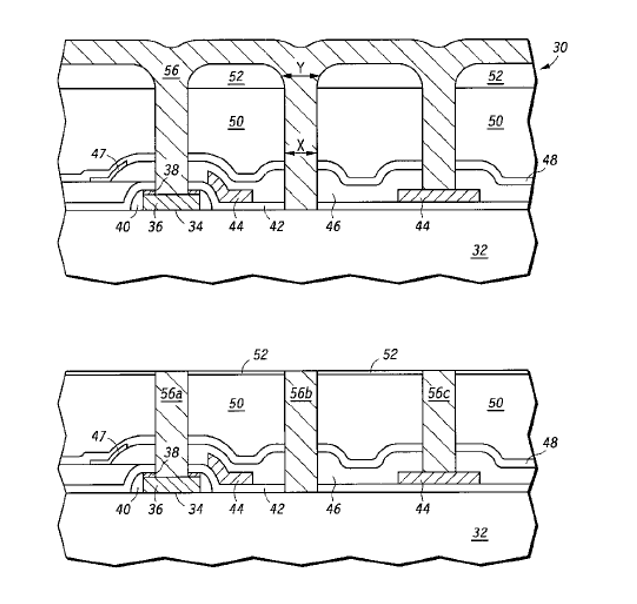
| etching the top surface portion of the dielectric layer adjacent the sidewall portion to form a taper that extends between a top surface of the dielectric layer and the sidewall portion, 蝕刻該介電層中與該側牆面相鄰的上表面,以形成一個延展該介電層的上表面與該側牆面之間的錐體, wherein the taper towards the top surface portion has a radius Y and the taper towards the sidewall portion has a radius X wherein X<Y; and 其中,該指向該上表面部份的錐體的半徑為Y,且指向該側牆面的錐體的半徑為X,又X小於Y;以及 |
| removing remaining portions of the resist layer; 移除該抗腐蝕層剩下的部份; |
| depositing a second conductive material within the opening; and 沈積一個第二導電材料於該開口;以及 |
| polishing away a top portion of the conductive material and a top portion of the dielectric layer to remove the taper. 將該導電材料的一個頂部及該介電層的一個頂部拋光掉,以移除該錐體。 |
表十一、申請專利範圍解析
| US6,492,686 Claim1 |
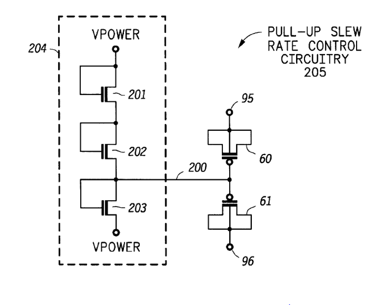
| 1. Circuitry formed on an integrated circuit, the circuitry comprising: 一個形成於一積體電路的電路,該電路包含: |
| a first terminal; a second terminal; 一個第一端;一個第二端; |
| a first transistor having a first body, a first control electrode, a first source region, and a first drain region, wherein: 一個第一電晶體,其包含一個第一主體,一個第一控制電極,一個第一源極,一第一汲極,其中: the first body, the first source region, and the first drain region are shorted together and are coupled to the first terminal; and 該第一主體,該第一源極,與第一汲極係彼此短路,且均耦接於該第二端;以及 |
| a second transistor having a second body, a second control electrode, a second source region, and a second drain region, wherein: 一個第二電晶體,其包含一個第二主體,一個第二控制電極,一個第二源極,以及一個第二汲極,其中: the second body, the second source region, and the second drain region are shorted together and are coupled to the second terminal, 該第二主體,該第二源極,與第二汲極係彼此短路且均耦接於該第二端, |
| the second control electrode is coupled to the first control electrode, and 該第二控制電極係耦接於該第一控制電極,且 the second transistor is of a same conductivity type as the first transistor. 該第二電晶體的導電類型係與該第一電晶體相同。 |
--------------------------------------------------------------------------------------------------------------------------------------------