2013年10月29日,日本光學電子零件商Enplas Display Device Corporation以及其美國分公司Enplas Tech Solutions, Inc.與Enplas (U.S.A.), Inc.(以下統稱Enplas),向美國加州北區聯邦地院提起請求確認之訴,請求法院確認韓國最大LED供應商首爾半導體公司(Seoul Semiconductor Company, Ltd.),其從美國大型集團公司Teledyne處所移轉取得之兩項與LED背光裝置相關的專利權利,未受到Enplas供應給其他LED照明設備廠之產品所使用的LED透鏡(lenses)零組件所侵害,且該兩項專利為無效。
Enplas在其訴狀中指出,在2013年10月16日,首爾半導體的委任律師寄送專利侵權警告函給Enplas,表示首爾半導體相信,本案2項系爭專利技術,與Enplas供應給諸如韓國LED照明設備廠Lumens Co., Ltd.與LG Innotek Co., Ltd.等、用於其LED產品中的透鏡等產品高度相關,而Enplas之行為就該2項專利構成誘使侵權與輔助侵權等間接侵權行為,因此首爾半導體要求Enplas立即停止其侵權行為並有意向美國聯邦法院或美國國際貿易委員會(ITC)尋求救濟。
Enplas認為,首爾半導體已表明意圖且準備向其提起專利侵權告訴,而在Enplas與首爾半導體間,就2項系爭專利權利是否受到侵害與其有效性等爭點存在爭議,是故其提起本案確認之訴。
本案2項系爭專利內容如下:
美國專利編號US 6,473,554,名稱為「小體積照明裝置(Lighting apparatus having low profile)」,於2002年10月29日核發,發明人為 David G. Pelka 與John Popovich,原始權利人為Teledyne Lighting and Display Products, Inc.,首爾半導體於2009年8月27日移轉取得本項專利權利;
美國專利編號US 6,007,209,名稱為「用來提供背光之光源(Light source for backlighting)」,於1999年12月28日核發,發明人為 David G. Pelka,原始權利人為Teledyne Industries, Inc.,首爾半導體於2013年9月26日移轉取得本項專利權利。(900字;表2)
表一、系爭專利之請求項解析
| US 6,473,554 請求項1 |
US 6,007,209 請求項1 |
1. An illumination device, comprising:
一項照明裝置,包括 |
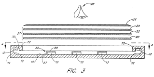
1. An apparatus (FIG.3 - 10) for backlighting a display panel (FIG.3 - 26), comprising:
一項用來提供顯示面板背光的裝置,包括 |
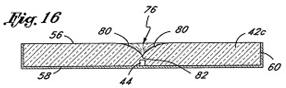
a waveguide (Fig.16 – 42c) having an illumination coupler embedded in an interior region of said waveguide,
一波導管,其具備嵌入前述波導管內部區域的一光耦合器 |
a housing (FIG.3 - 14) having a cavity formed by diffusively reflective bottom (FIG.3 - 15) and side surfaces (FIG.3 - 16), said housing having an aperture which opens into said cavity, said aperture configured to provide illumination to a rear surface of said display panel;
一外殼,其具備一由擴散反射之底邊與側邊表面所形成之空間,前述空間具備一開進前述空間的孔洞,前述孔洞被配置來提供照明給前述顯示面板的背面 |
said illumination coupler adapted to receive light from a point source (Fig.16 - 44) within said interior region, and to direct light between generally parallel top and bottom surfaces (Fig.16 – 56 & 58) outside said interior region,
前述光耦合器係用以從位在前述內部區域中之點源接收光線,並在位於前述內部區域外、大致平行之頂部與底部表面之間導引光線 |
a first series of light-emitting devices (FIG.3 - 12), mounted about a perimeter of the cavity;
第一系列之光線釋放裝置,被架設於空間周邊 |
said illumination coupler comprising a refractive index interface (Fig.16 - 80) which is inclined relative to at least one of said top and bottom surfaces said interface being configured to reflect light rays emitted by the point source which propagate along a line that forms less than the critical angle of total internal reflection with respect to a line lying in one of said top and bottom surfaces, such that light rays which would otherwise pass out of said waveguide are captured for propagation between said top and bottom surfaces.
前述光耦合器包括一折射率介面,其向頂部與底部表面至少其中之一傾斜,前述介面被配置來反射點源所釋放的光線,其沿著對在前述頂部與底部表面其中之一中的直線而言、以小於全內反射之臨界角的角度所形成的直線來傳導,藉以讓原本會逸出前述波導管的光線、被捕捉來在前述頂部與底部表面中傳導 |
a second series of light-emitting devices (FIG.3 - 13), mounted in a predetermined pattern on said bottom surface of said cavity;
第二系列之光線釋放裝置,以預定之模式被架設在前述空間的前述底邊表面 |
a diffuser (FIG.3 - 20) mounted across said aperture, so as to diffuse illumination which passes through said aperture from said cavity toward said display panel;
一散光器,其被架設橫跨在前述孔洞上,藉以擴散從前述空間朝向前述顯示面板而經過前述孔洞的照明光線 |
a brightness enhancing material (FIG.3 - 22) disposed between said diffuser and said display panel, said material concentrating illumination within a viewing angle so as to enhance the brightness of the display panel; and
一亮度提升物質,其位於前述散光器與前述顯示面板間,前述物質聚合照明光線於一視角內,藉以提升顯示面板亮度 |
said housing further comprising shielding elements (FIG.3 - 58) positioned relative to at least some of said light emitting devices of said first and second series such that light emitted by the shielded emitting devices is substantially uniformly distributed throughout said cavity, whereby hot spots in said display panel are effectively eliminated.
前述外殼進一部包含遮蔽元件,其相應於至少部分前述第一與第二系列光線釋放裝置而被置放,藉以讓受其遮蔽之光線釋放裝置所釋放之光線、可以相當一致地在前述空間內散佈,進而有效消除前述顯示面板中的熱點 |
 |
 |
Source: 科技政策研究與資訊中心—科技產業資訊室整理,2013/11
表二、專利訴訟案件基本資料:
Enplas提起請求確認首爾半導體專利無效與未受侵權之訴
| 訴訟名稱 |
Enplas Display Device Corporation et al v. Seoul Semiconductor Company, Ltd. |
| 提告日期 |
2013年10月29日 |
| 原告 |
Enplas Display Device Corporation
Enplas Tech Solutions, Inc.
Enplas (U.S.A.), Inc. |
| 被告 |
Seoul Semiconductor Company, Ltd. |
| 案號 |
3:13-cv-05038-NC |
| 訴訟法院 |
the U.S. District Court for the Northern District of California |
| 系爭專利 |
US 6,473,554
US 6,007,209 |
| 系爭產品 |
Enplas所生產、用於其他廠商(如韓商Lumens與LG Innotek等)之LED照明產品中的LED透鏡,
http://www.enplas.co.jp/english/business/led_product/ (最後瀏覽日:2013/11/07) |
| 訴狀下載 |
 |
Source: 科技政策研究與資訊中心—科技產業資訊室整理,2013/11
2016
- 09-02首爾半導體勝訴 日企Enplas專利無效且須付407萬美元授權金
-
原告: 首爾半導體 v. Enplas
在美國、歐洲、韓國、台灣等地提起的“專利無效”訴訟全部勝訴,Enplas公司提出專利全部被判無效。
美法院就Enplas公司故意侵犯首爾半導體透鏡兩項專利(US6007209、US6473554)判決,共需向首爾半導體支付一次性專利合理授權金407萬美金。
這場全球專利戰由首爾半導體佔上方。起始從2013年Enplas公司先主動控告首爾半導體背光透鏡專利無效開始,這場專利保衛戰愈演愈烈。首爾半導體隨後發起強烈反擊,在美國、韓國、歐洲及台灣對Enplas提起專利無效訴訟,2015年7月20日,歐洲專利局判決Enplas公司專利無效,之後Enplas向美國上訴法院提起上訴但被駁回。
首爾半導體對Enplas公司在美國提起的專利侵權訴訟也取得勝利。2016年8月10日,美國聯邦法院認定首爾半導體專利有效,最終判決Enplas公司故意侵犯其專利,賠償首爾半導體407萬美元。
另外,首爾半導體在2014年7月,對使用Enplas公司透鏡的北美TV製造商Craig和Curtis兩家公司提起5項專利侵權訴訟,包括EPI、芯片、封裝、LCD用背光透鏡及構造相關專利,最終確認侵權成立之後,雙方達成授權和解。首爾半導體計劃在歐洲等國家也提起專利使用費及損害賠償訴求,對使用Enplas公司透鏡的企業提起追加訴訟。
--------------------------------------------------------------------------------------------------------------------------------------------